Custom ESP32-based PCB
Skills required
PCB & Circuit Design
Software Development
Manufacturing
The Why
Unfortunately, I am not able to say too much regarding this project as it is a part of something we are currently working on at Neucin, my workplace, however I wanted to show off a some of my PCB design capability!
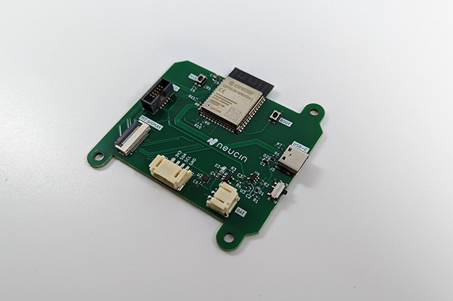
The purpose of the custom PCB design was to consolidate an initial prototype electronics design and enable it to be integrated into a compact user-friendly case. The PCB design incorporates an ESP32-S3 microcontroller, which offers WIFI and Bluetooth connectivity, a USB-C port for charging and firmware flashing, battery charging and monitoring functionality, a board-to-board connector for interfacing with a sensor and a FPC connector for seamless connection to a TFT capacitive touch screen.
The How
Before I began researching the components it was important to define the requirements for the custom PCB, considering factors such as size, functionality and integration with the enclosure. Once these requirements were defined, I was then able to identify suitable components such as the linear voltage regulator and battery charging circuitry. For the microcontroller I selected a ESP32-S3 as this comes with integrated Wi-Fi and Bluetooth and does not require a USB to serial converter, meaning fewer components. I was also keen to integrate a USB-C connector due to its user-friendly design.
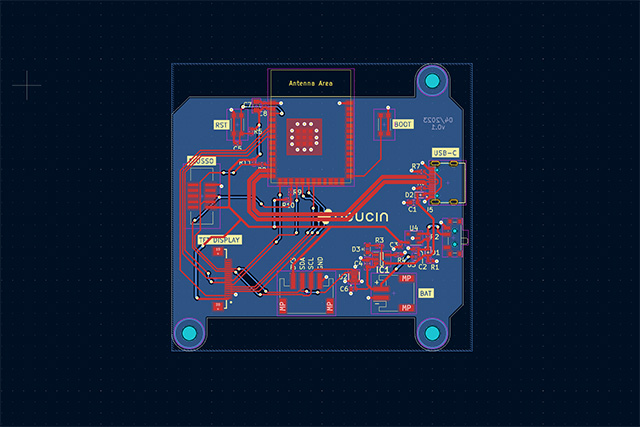
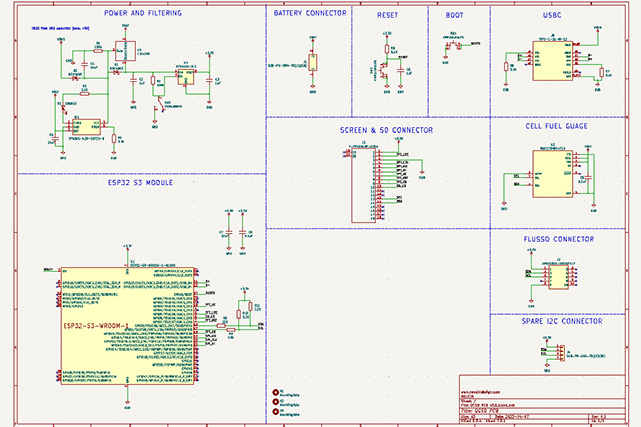
Once I had the key components selected, I was able to start with the schematic design. For this I utilised KiCAD, a free and open-source PCB design software, and its Schematic Editor. Once I had completed the schematic, KiCAD allows the schematic design to be easily transferred to the PCB layout stage. As we had defined the requirements of the size of the PCB and how it would integrate into the casing early on, it was easy to determine the overall PCB dimensions. From there I was able to begin placing components, keeping in mind ease of assembly and considering how the traces would be routed. With the majority of the components in their rough location I was able to begin routing the traces, ensuring the proper clearance and tweaking the location of the components where necessary. The use of a ground plane on the bottom layer made routing to ground much easier. In addition to this, I had to select the correct trace width for the power it would carry and ensure the USB differential pair met the impedance requirement of the USB specification. After I had the components placed and the traces routed, I was able to place the mounting holes and begin thinking about manufacturing.
For manufacturing and assembly of the PCB I chose JLCPCB as they were cost effective and offered a short lead time. Before exporting any gerber files, based on the capabilities of JLCPCB, I made sure to review and verify the PCB design for any errors or potential issues, utilizing KiCADs design rule checks (DRC) and electrical rule checks (ERC). Once I was confident in the PCB design, KiCAD makes it easy to export the gerber, drill and pick and place files which can then be uploaded to JLCPCB along with a BOM to be manufactured. From there it was just a matter of waiting!
The Outcome
After a week filled with anticipation, I received the fully assembled PCBs and I am happy to say everything worked as expected! I was really happy with how the PCB came out as this was a big setup in complexity compared to PCBs I had designed in the past. Luckily, I wont have to wait long to design my next PCB as we already have a plan for the next revision which includes even more features!


